GPU EM Solver
GPU-accelerated FDTD solver matching CST/MATLAB accuracy. Reduced simulation time of a 4x4 array from 222h (CPU) to 6.8h (GPU).
GPU-Accelerated Electromagnetic Wave Solver
Technical focus
- Build a GPU-first FDTD solver that can handle my 5.4GHz 4x4 patch array when CST/HFSS/OpenEMS cannot.
- Stay bit-for-bit matched to a single threaded CPU reference while validating against CST Microwave Studio, Mathworks RF PCB Toolbox, and analytical microstrip cases.
- Optimize memory bandwidth with a structure-of-arrays layout, coalesced access, and Nsight-informed kernel optimization.
- Benchmark both MUR and PML8 boundaries and run a broad PCB-focused validation suite before multi-GPU tiling.
- Plan radiation capture, dedicated per-region kernels, and multi-GPU domain splitting after the single GPU path is fully optimized.
Results
- 17 GCell/s (28x faster) with MUR and 6.5 GCell/s (32x) with PML8 on a 5070 Ti vs OpenEMS on a Ryzen 9950X.
- For the 4x4 patch array saw a drop from 222 hours in OpenEMS to 6.8 hours on my solver.
- Outputs match my CPU reference while reproducing CST Microwave Studio (bandpass filter) and Mathworks RF PCB Toolbox (bandstop filter).
- Validated six benchmark geometries with research/Mathworks overlays and rendered fields in ParaView; solver scales well with GPU memory bandwidth.
Stack
Performance vs. State of the Art
OpenEMS is unacceptably slow. On a modern Ryzen 9950X CPU, it runs my benchmark cases at roughly 200MCell/s (using proper PML boundary conditions).
In contrast, my custom solver running on an $800 consumer graphics card (5070 Ti) achieves:
- 17GCell/s, 28x faster, using approximate MUR boundary conditions
- 6.5GCell/s, 32x faster, using proper PML8 boundary conditions
This represents a collapse in simulation time from 222 hours (a week and a half) down to 6.8 hours (same day results).
With open-source software clearly crushed, the gloves are coming off, and I'm going after a comparison to the world's current fastest FDTD EM solver - Empire XPU. Empire XPU is a commercial software out of Germany, produced and maintained by IMST GmbH. They regularly post speed records on Linkedin using ludicrous setups such as dual 128-core Epyc CPUs with speeds peaking just under 150GCell/s [link] .
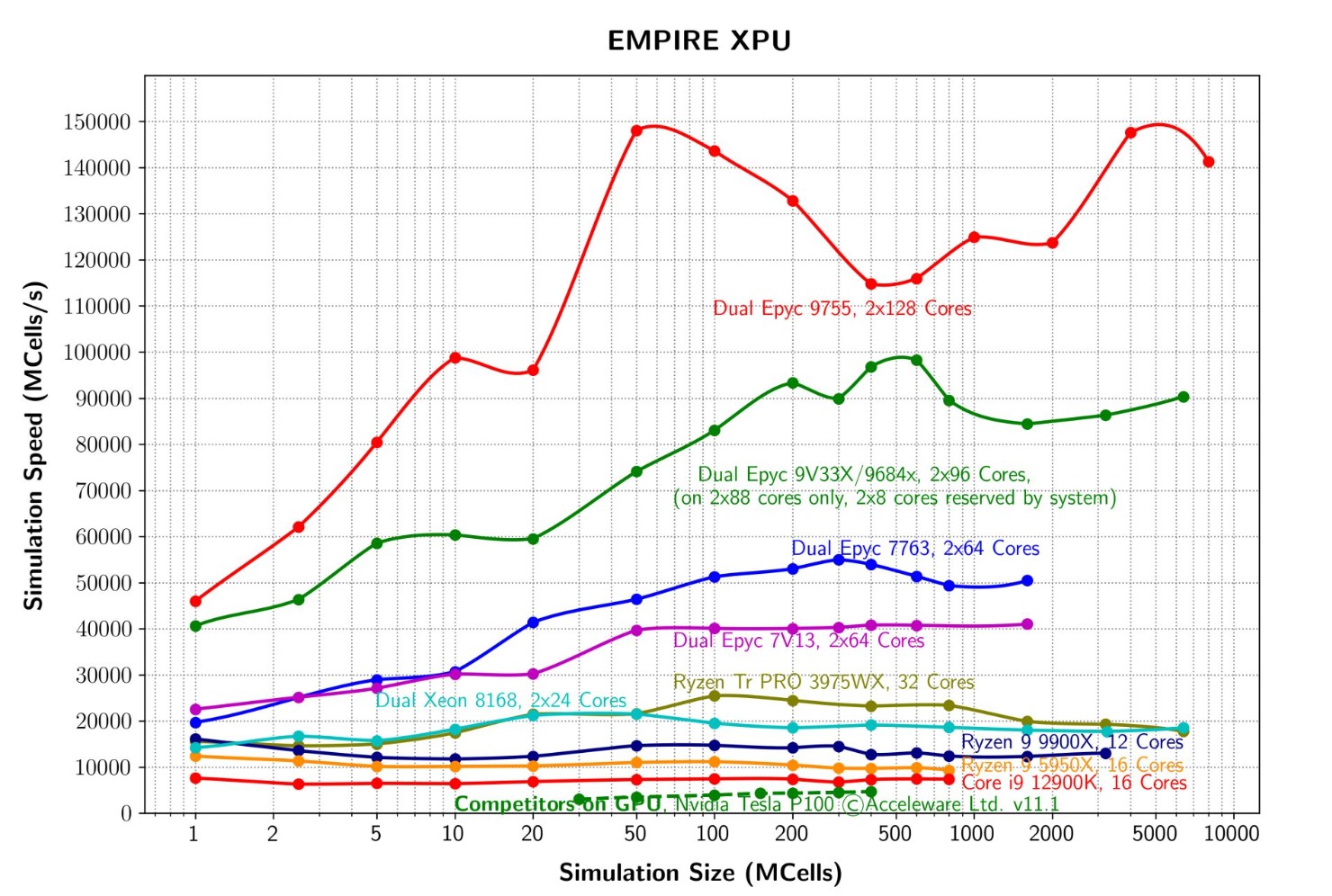
For reference, that CPU setup costs (NOT including any RAM or motherboard, etc), around $26,000USD. Given the hardware component driving my speeds is 32x cheaper, but my code is only 9x slower, and parallelizable, I smell blood in the water.
Unlike OpenEMS, my solver scales with GPU memory bandwidth which is one of the fastest growing performance metrics in hardware, can be split across GPUs to further multiply speed.
Validating my solver's accuracy
Speed means nothing if the math is wrong. Before setting any world-records, I had to validate that my solver is producing CORRECT outputs, not just randomly mashing around cells really quickly.
I executed a solid plan to accomplish this - first set up a benchmark suite of multiple "standard" microwave circuit geometries with well-known analytical solutions, and second reproduce at least 1 non-trivial result from an EM/RF research paper and 1 non-trivial result from a commercial solver.
| Benchmark / reference | Preview |
|---|---|
| 6GHz microstrip patch antenna | 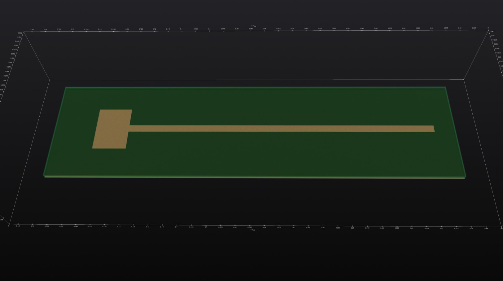 |
| 6GHz microstrip patch antenna with quarter-wave transformer feed (QWT) |  |
| Open microstrip |  |
| Microstrip with open stub on the side | 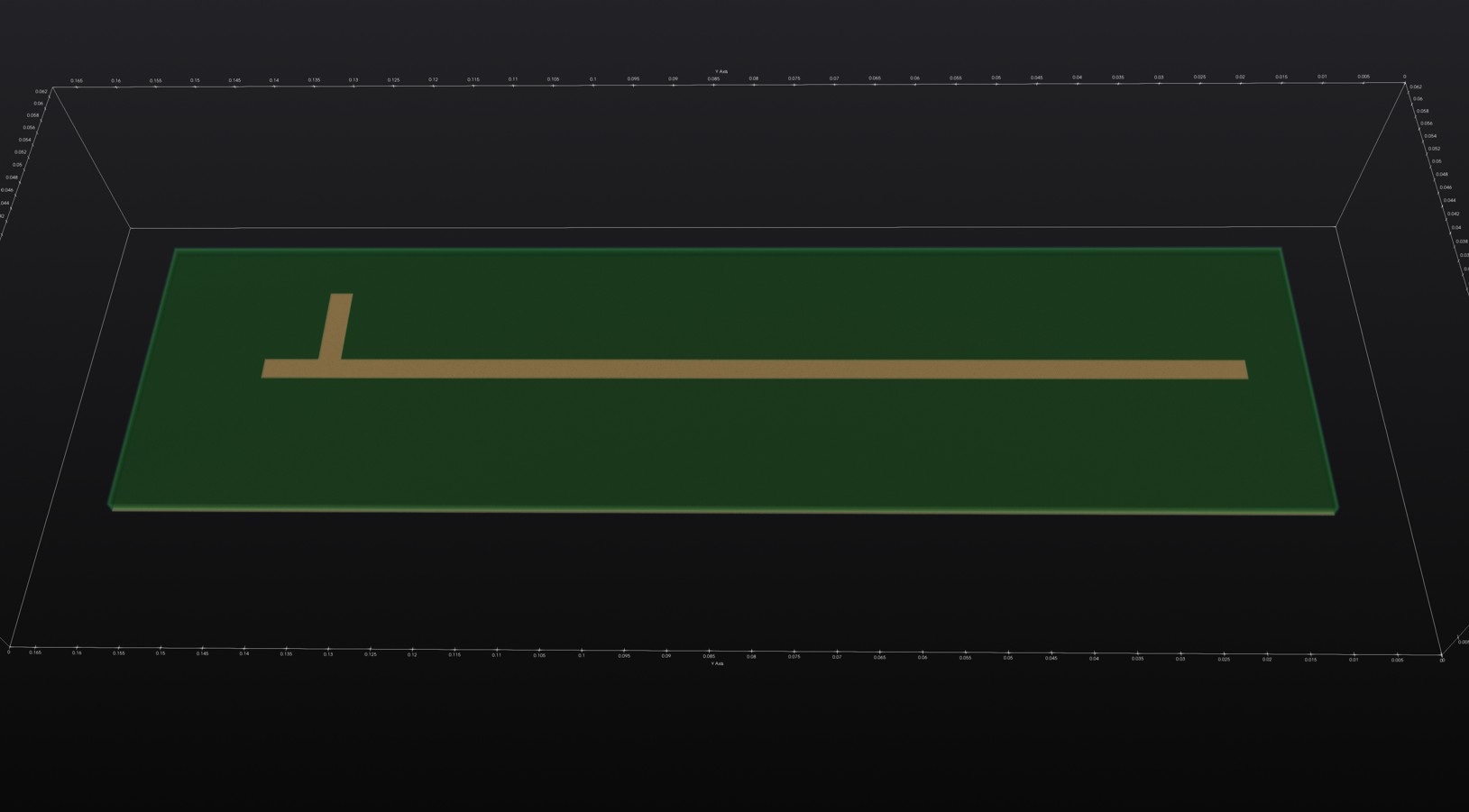 |
| A research paper optimizing a microstrip coupled bandpass filter using CST Microwave Studio. [link] | 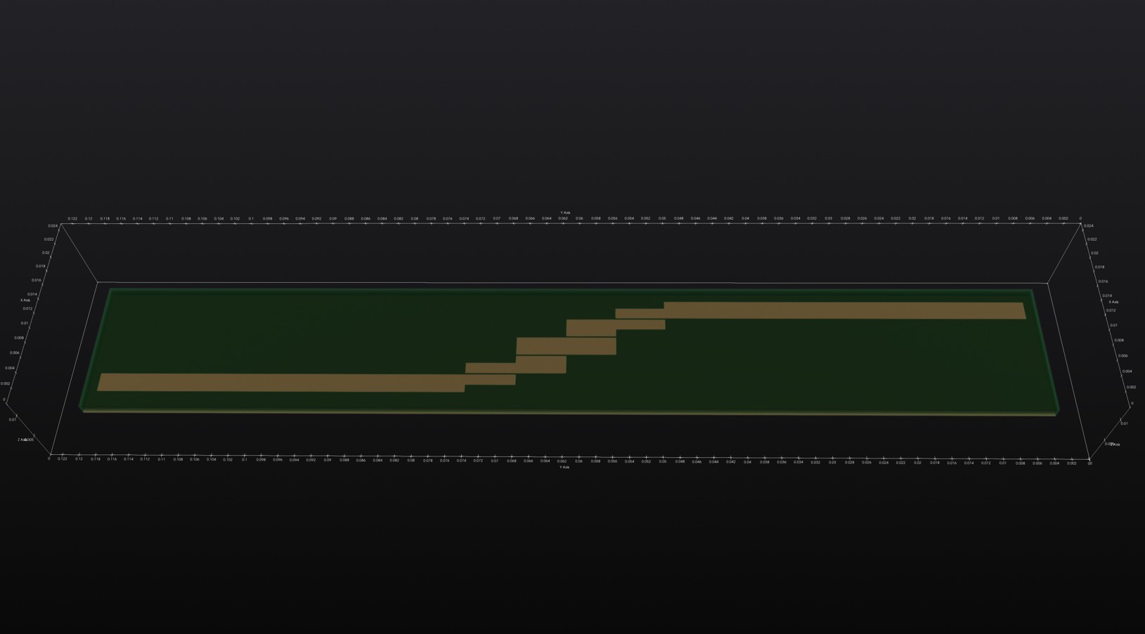 |
| An official example from Mathworks which applies the MATLAB RF PCB Toolbox to evaluate an open stub-based bandstop microstrip filter. [link] | 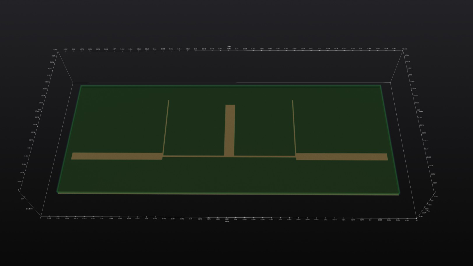 |
I will state the obvious - all of these benchmarks only test planar PCB structures. This is because of two reasons, 1) my actual use case for this solver is mostly PCB simulations, and 2) it's easier to use analytical equations to predict planar structures than arbitrary geometry, so validation becomes more reliable. However, the solver has absolutely no internal limitation on the geometry structure.
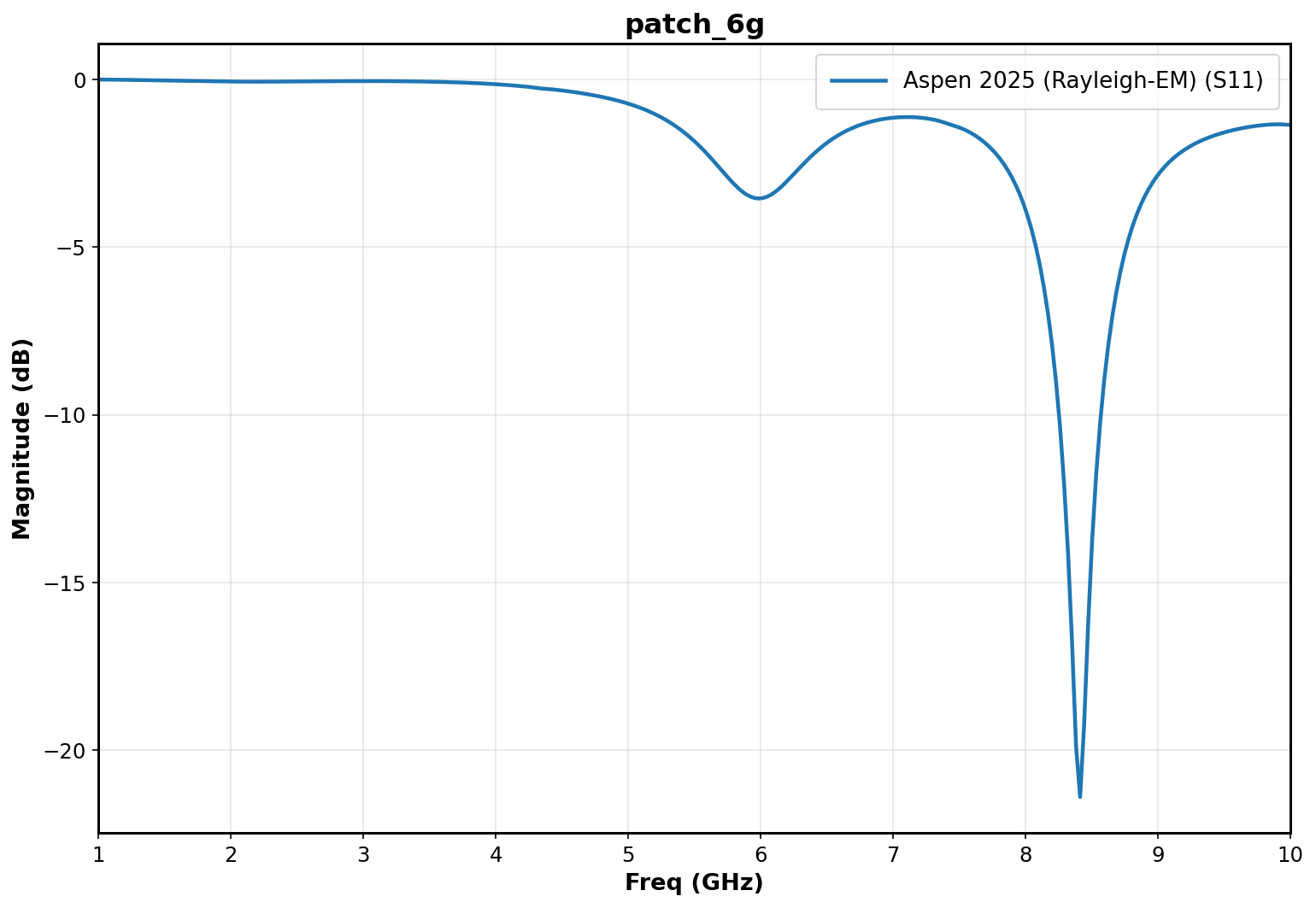
Benchmark 1: 6GHz Microstrip Antenna
We expect a dip in S11 at 6GHz. In the plot below we observe precisely this trend, with a second resonance higher up in frequency.
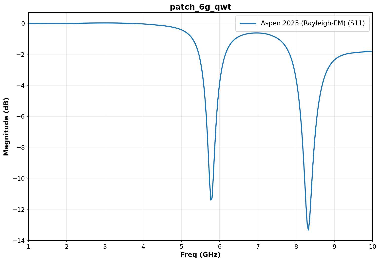
Benchmark 2: 6GHz Antenna w/ Quarter-Wave Transformer
The same 6GHz antenna now paired with a QWT matching strategy should exhibit much better S11 at the target frequency of 6GHz. The plot below precisely confirms this expectation.
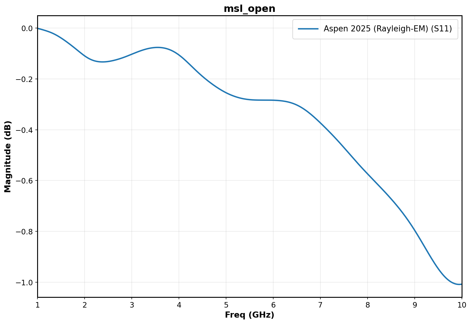
Benchmark 3: Open Microstrip
For an open microstrip geometry we expect a flat response of nearly 0db at lower-medium frequencies. Higher frequencies will see attenuation in S11 as the open microstrip edge behaves like an antenna.
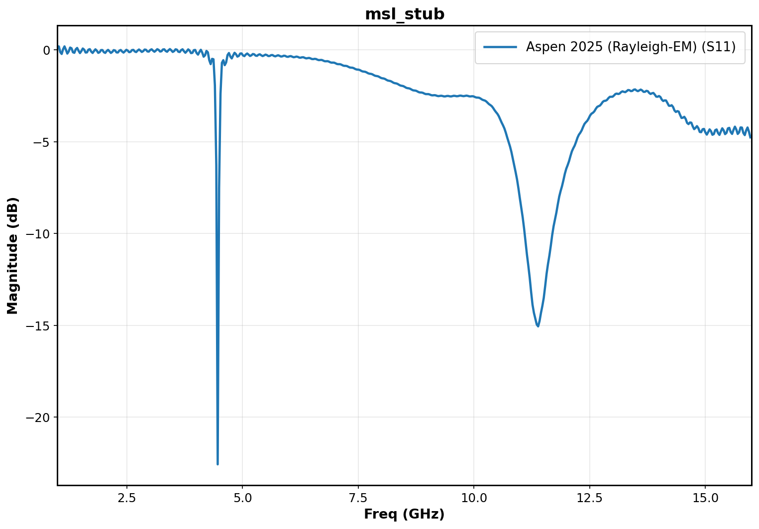
Benchmark 4: Microstrip Stub
Considering a stub characteristic length of 10mm feed coming off a 2.67mm wide feed we can expect interesting effects near the characteristic quarter wave length (8.7mm, the distance from the stub edge to center of feed due to how geometry is defined). A quick hand calculation shows the quarter wave frequency with eps_r =4.5 and h=1.5mm is 4.7GHz:
And inspecting our plot below, we see a sharp dip in S11 precisely near 4.7GHz, with a second resonance higher up in frequency. Fantastic.
Replicating Research: 5-7GHz Coupled Bandpass Filter vs CST Microwave Studio
In this research paper "Designing a Microstrip coupled line bandpass filter", [link] the author (Ragani Taoufik) presents a design with excellent wideband performance between 5-7GHz for WLAN and other applications.

I extracted the numerical points from Ragani Taoufik's work into a csv file using WebPlotDigitizer. Finally, running the geometry through my simulator with the same material properties as described in the paper we obtain the comparison S11 plot below:
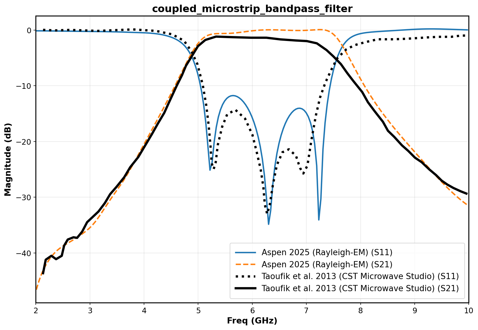
Inspecting the plot, we see a near identical match in outputs between CST and my solver. Overall, excellent match to the reference.
Replicating Industry: Open Stub Bandstop Filter vs MATLAB RF PCB Toolbox
Mathworks provides official usage examples for their RF PCB Toolbox. I set up the presented geometry in my solver, and used WebPlotDigitizer to save the MATLAB result as CSV to overlay with my output.
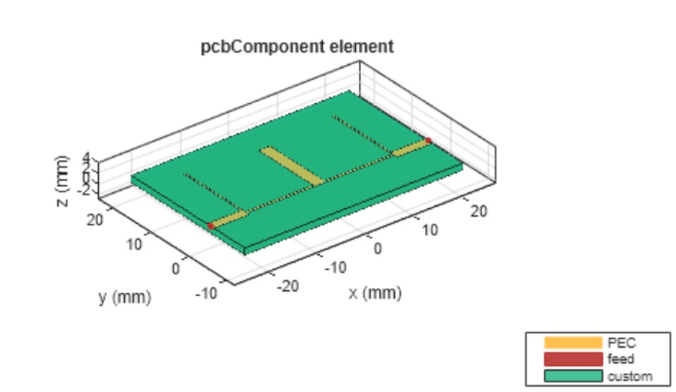
Running the solver with the presented material properties and board stackup, we obtain the following S11 comparison plot:
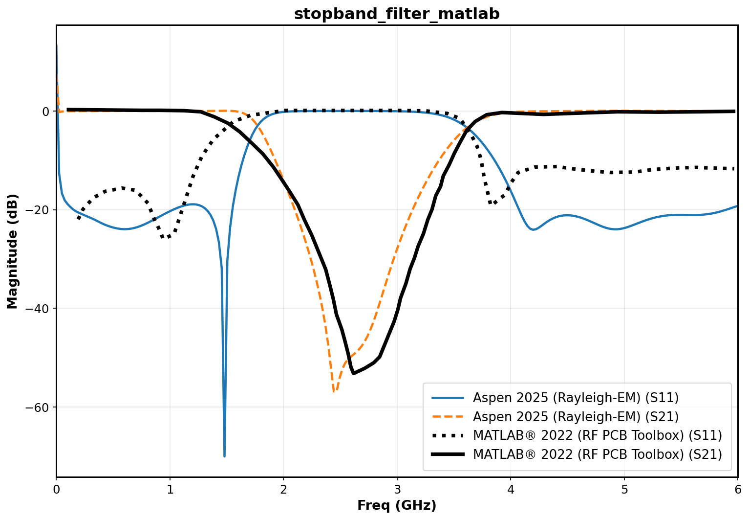
Comparing the plot results, we can see that my solver mostly agrees with RF PCB Toolbox in the areas of bandwidth, frequency range and S11 magnitude. There is an apparent frequency offset in the S21 dip and S11 flat area in the stopband of a few hundred MHz. The exact reason for this disagreement is not clear to me, but given that my solver agrees well with CST I am inclined to believe that my solver is actually more correct than the RF PCB Toolbox in this instance.
Project Origin: The "Why"
With the performance and accuracy established, I want to explain why I started this project in the first place.
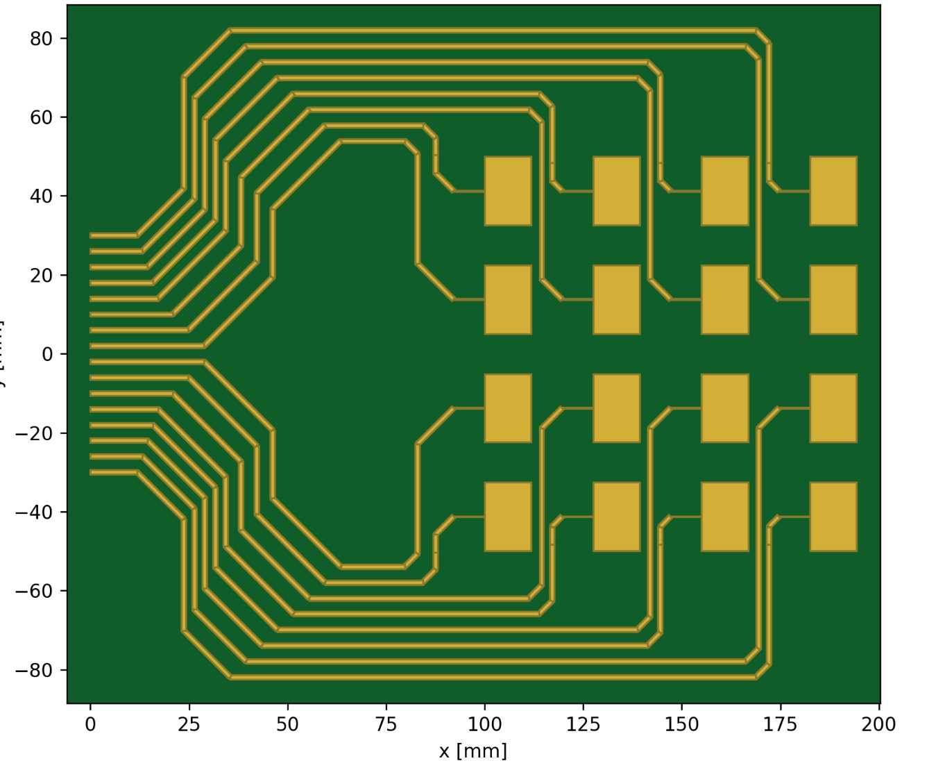
After my first real RF project, my FMCW radar, I wanted to make an improved version using a high gain patch antenna array on-PCB rather than externally mounted, and I also wanted to nearly double the frequency to 5.4GHz. With these goals in mind, I looked for a suitable software package to simulate the radiation patterns, and scattering parameters. As a student at U of T my first choice was ANSYS HFSS - but after downloading and trying to build my problem I quickly found that the student-license limitations were too strict, the number of mesh cells permitted simply couldn't describe my 16-element 4x4 array, pictured below.
So, in search of an open source alternative I settled on "OpenEMS" [link], which has no artificial domain or resolution limitations. OpenEMS is a neat project, and I spent ~1 month learning how to use the Python interface and optimize my problem definition to simulate up to a 2x2 patch antenna array at my desired frequency. The video below shows the surface current density on a 2x2 patch antenna array I simulated.
However, because OpenEMS runs on CPU-only, unfortunately my 5.4GHz, 4x4 patch antenna array is still out of reach. To put the computational cost in perspective:
- 200mm x 200mm x 40mm = 2500 cells x 2500 cells x 500 cells
- 1.6 Billion cells
- Assume we need 100k timesteps for the structure to ring out fully
- 160 Trillion cell updates required
- Assume 200MCell/s rate (OpenEMS peak)
- 222 hours = a week and a half running at max speed just to get one result.
That's when I decided - I need to make my own EM solver built for GPU-first with aggressive optimization, while ensuring results match industry standard tools.
Implementation Details & Theory
I used multiple textbook references and wrote my solver from first principles - not polluting my mind with implementation-specifics of other solvers. The first implementation was a very basic C++ program running single threaded on the CPU to set a functional baseline, and then I scaled to CUDA GPU shortly after getting that working.
Brief background on the FDTD method
OpenEMS uses an approach called Finite-Difference Time-Domain (FDTD). By injecting a broadband pulse excitation into microwave structures the return reflections can be measured, and a Fast Fourier Transform (FFT) performed to recover the response over ultra wide frequency bands. The core principle of FDTD relies on the Yee cell grid structure, where the magnetic field components sit on cell faces, and electric field components sit on cell edges. The diagram below (not mine!) illustrates this principle.

Starting with Maxwell's equations:
And define a standard Yee grid with time staggering where E and H updates are offset by half a timestep. More explicitly, define the grid as:
And discretize the update equations for each cell as follows:
Electric field update
Where \(c_u\) are pre-calculated coefficients combining \(\Delta t\), \(\varepsilon_0\), \(\varepsilon_r\), and the cell dimensions.
Magnetic field update
Where \(tMU\) are pre-calculated coefficients combining \(\Delta t\), \(\mu_0\), and the cell dimensions.
What actually makes my solver so fast?
As you can see, the update equations are arithmetically light (add, subtract, some multiply), but very memory-heavy, since we need to stream each field component of all cells into the CUDA thread each timestep. The memory access and bandwidth bottleneck is a critical highlight as to why GPUs are well suited to this task.
My core design principles for the CUDA GPU implementation were:
- Maintain bit-for-bit reproducibility to the single threaded CPU version
- Maximize coalesced memory access
- Maximize total memory throughput
- Use Nvidia Nsight Compute to profile, analyze, and iterate
Achieving optimal coalesced memory access and pushing higher (useful) memory throughput on the GPU led me down a fun rabbit-hole of optimizing my core update kernels and memory layout, which I eventually settled on using a Structure of Arrays (SoA), with one array for each field component.
I have considered commercializing this solver in some capacity due to its very high performance relative to open source and even commercial options, hence I will not disclose further details about GPU-specific optimization strategies.
The next leap: Multi-GPU tiling
My sights are set on achieving a cell update speed higher than any posted by Empire XPU. I plan to accomplish this by implementing multi-GPU tiling where the simulation space is split across each device and some data is exchanged over the PCIe (or NVLink) bus between frames to synchronize the virtual boundary.
However, before implementing the exciting multi-GPU tiling I am determined to work on a few aspects of the solver that will become harder to implement after multi-GPU tiling if I don't do them first:
- Radiation pattern capture using a Huygens surface for more antenna characterization
- Dedicated kernels per-region (optimized codepaths, less branches)
- Diamond time-space tiling (uncertain payoff because of added overhead, but want to explore)
- Optimize register/L1 cache reuse when rolling kernels along a particular axis
After I have (at least attempted) the above, I will begin work on automated domain subdivision across devices, virtual boundary synchronization, and output consolidation. This writeup will be updated after all of that is completed, not incrementally.
Reach out over email (Contact button) if you are interested in licensing my algorithms or hiring me😉.