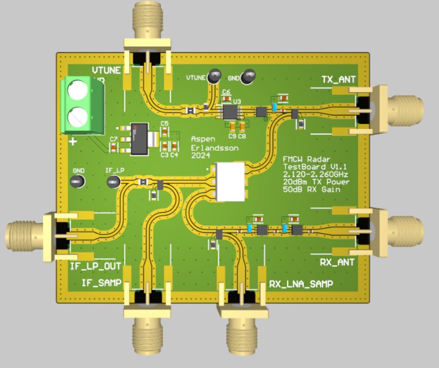
FMCW Radar PCB
2.0-2.4GHz FMCW radar on a 6-layer GCPW PCB with tuned Yagi antennas. Validated RF performance using a spectrum analyzer and VNA.
FMCW Radar PCB
Technical focus
- 2.0-2.4GHz FMCW radar on a 6-layer impedance-controlled stackup with VCO, PA, LNA chain, mixer, and LPF.
- Designed and tuned paired Yagi-Uda antennas with a calculator and VNA, mounted on a 3D printed structure.
- Selected RF passives via Murata Simsurfer, curved GCPW traces, and used bias networks to manage gain and noise.
- Bench validation with a TinySA, function generator sweep, and oscilloscope.
Results
- Assembled via stencil and hotplate; validated the signal source and PA on a TinySA before full chain tests.
- Sawtooth VCO drive produced the expected wideband sweep; mixer IF shows distance-varying sine vs the wall target.
- Antennas tuned after printing; VNA confirmed matching and link budget assumptions.
- Planned next steps: on-board DSP/MCU and integrated patch array to remove external antennas.
Stack
System Overview
This project realized my goal of building a frequency-modulated continuous-wave radar (FMCW) operating between 2.0-2.4GHz. The system is built on a custom 6-layer impedance controlled stackup integrating a voltage controlled oscillator (VCO), a power amplifier, multiple low-noise amplifiers (LNAs), a mixer, and low-pass filter.
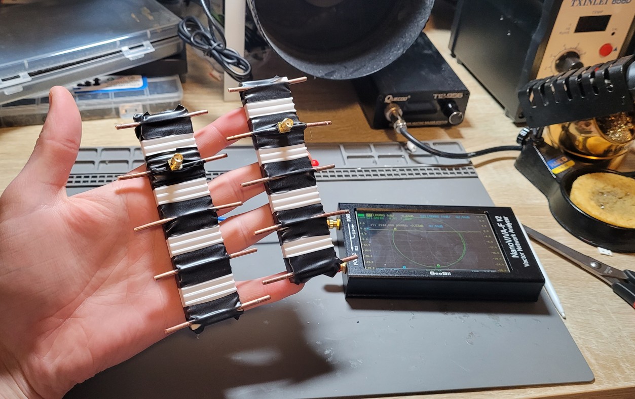
Using analytical equations and CAD (3D printing), I designed two identical externally connected high-gain Yagi-Uda antennas for the transmit and receive paths of my radar board.
Hardware Validation & Results
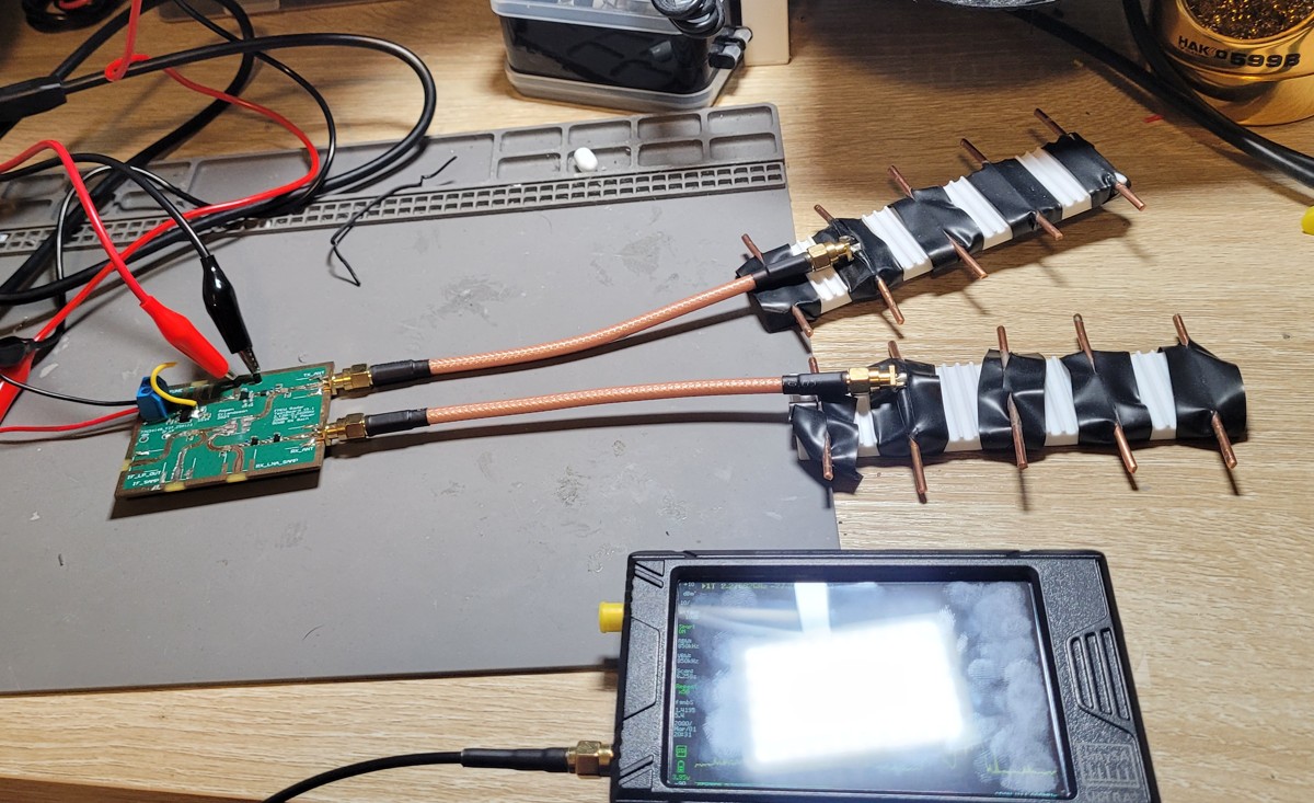
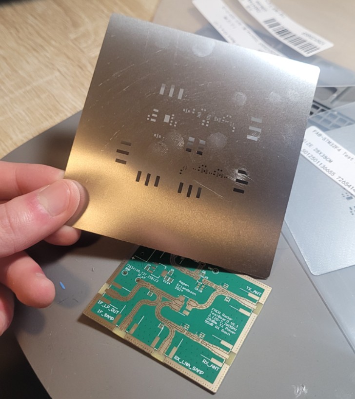
By the time the board arrived for assembly, I had plenty of experience assembling advanced PCBs by hand through UTAT Rocketry. I used a RoHS solder paste with a stencil and framework jig so dispense the paste on each pad, and tweezers to place components. Using a hotplate I reflowed the board and inspected for any defects.
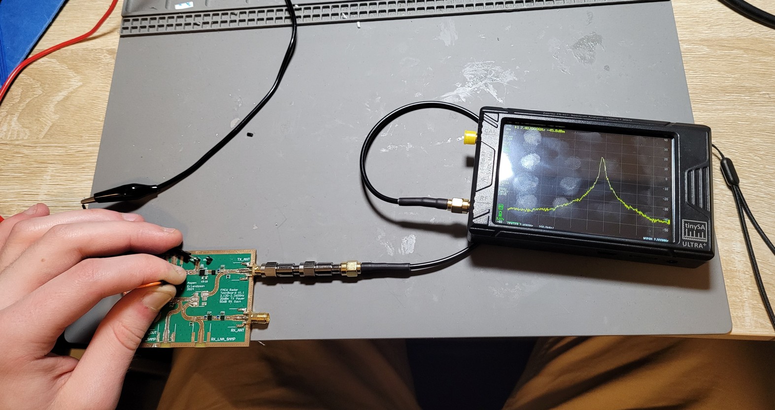
Once assembled, I powered it on using my programmable power supply and measured the output feed power level and frequency using my TinySA spectrum analyzer. This confirmed that the signal source and power amplifier were behaving as expected. Using my arbitrary function generator I produced a sawtooth signal and observed a very wideband power output on my spectrum analyzer as expected.
Because my frequency band was not exactly WiFi, and deliberately a few hundred MHz lower, I had to make my own antennas. Using an online calculator Yagi antenna design calculator I generated initial design parameters and 3D printed a structure to hold the copper elements. Because I had a Vector Network Analyzer (VNA), I knew I would be able to tune the design after making it, so I designed-in adjustable element placement from the start.
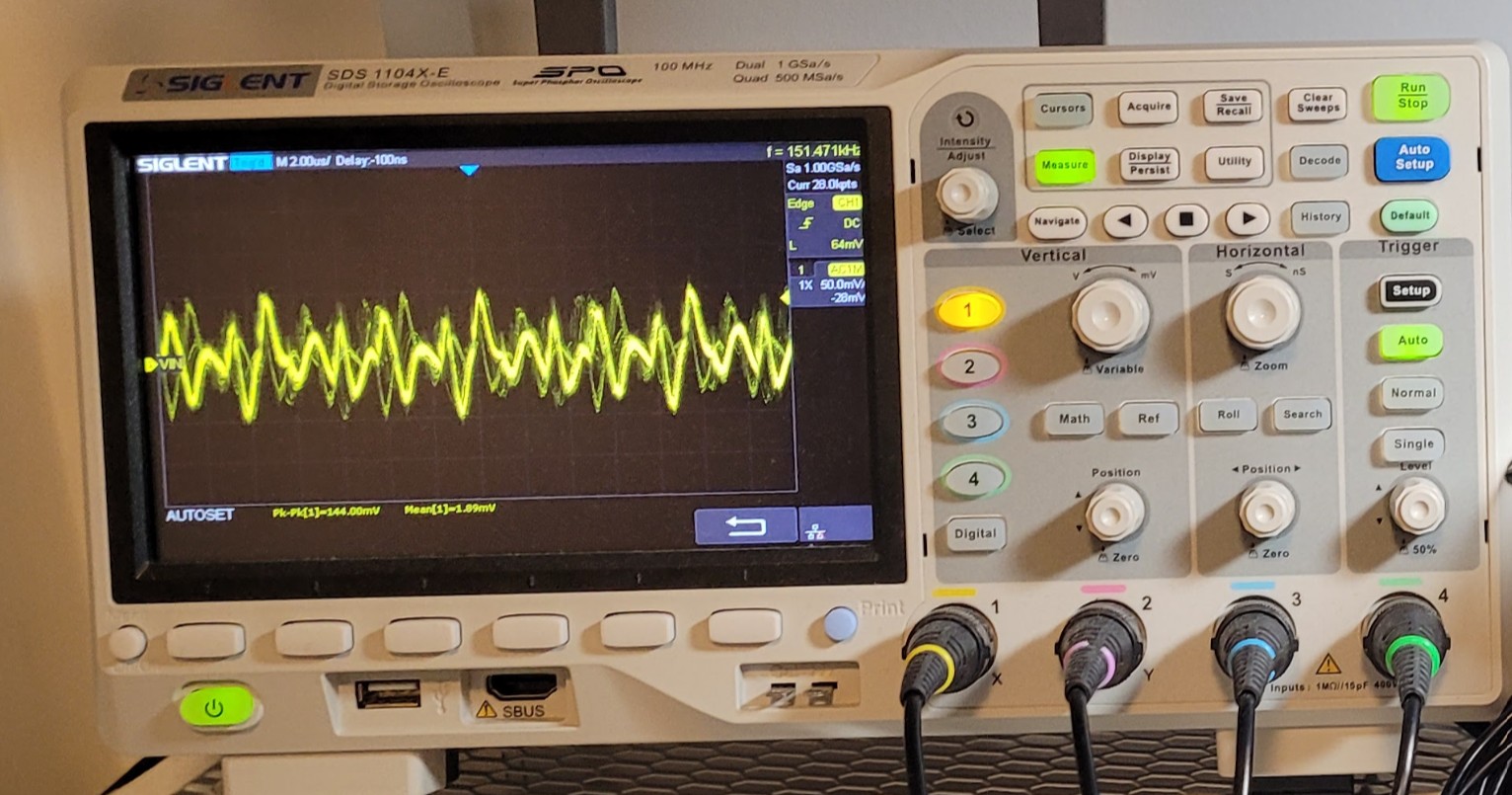
After printing and tuning the two antennas it's time to put everything together and power on the system. At the time of writing I rent a basement room which makes testing easy - the walls have earth and stone behind them which strongly reflect 2.2GHz signals and have a high effective radar cross section. I used my function generator to create the same sawtooth VCO drive signal, and measured the output from the mixer using my oscilloscope. As expected I measured approximately a sine wave with frequency varying with how close the antennas were from my observed object (the wall).
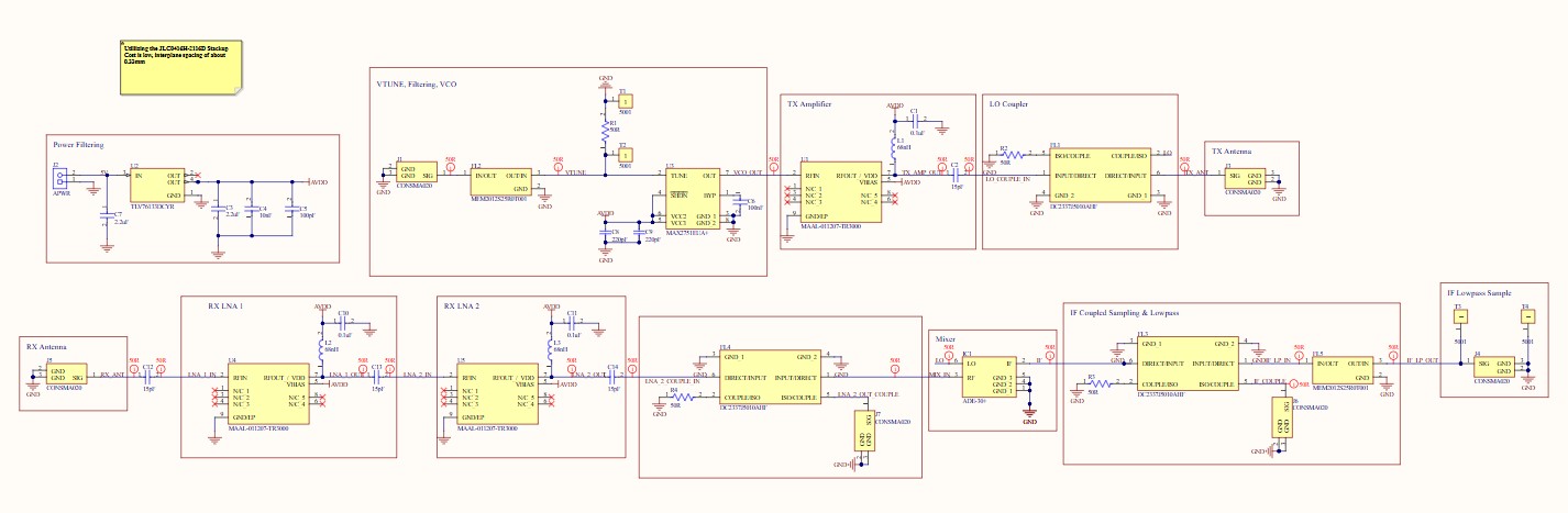
PCB Design & Implementation
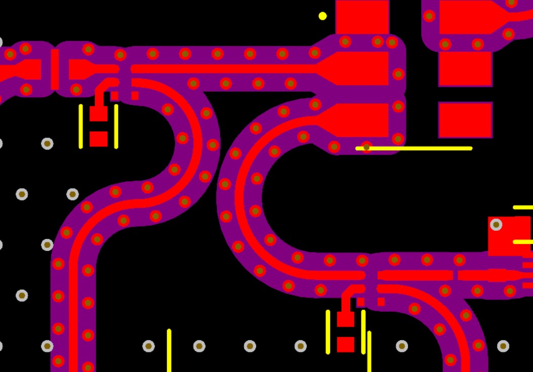
I used Altium Designer for schematic design and layout. Many RF principles were considered during both component selection, and layout:
- Power levels stack up between components.
- SNR/Link budget based on typical radar cross sections, LNA noise figure, etc.
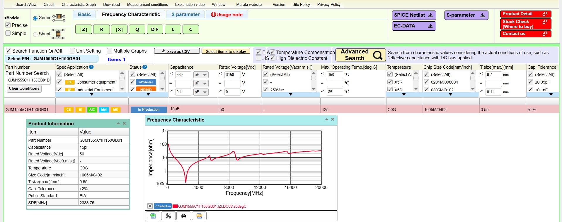
- SRF/Parasitic properties of passive components used. I referenced MuRata Simsurfer to carefully select appropriate capacitors.
- Bias networks for amplifier power.
- Low noise power source design.
- Impedance matching traces.
- Smoothing corners, pad interfaces, etc. to minimize reflections.
- Grounded co-planar waveguide (GCPW) microstrips to reduce coupling across traces while ensuring correct impedance.
Once the design was finished I did what all good designers do - ask for review from someone more skilled. After implementing some feedback from my electronics mentor regarding component/pad size (use 0402 in some places instead of 0603 as the pad size better matches the trace), I sent the board off for manufacturing.
Project Origin & Theory
After over half a year in the position of Avionics Lead on the University of Toronto Aerospace Team (UTAT) Rocketry, I felt drawn to engage with a more challenging design space - high frequency RF. The highest frequency system on-board our rocket is a GPS receiver, which almost doesn't count since the only design work required is routing a single impedance-matched trace from the SMA connector into the GPS module.
I wanted to build a radar system for a while, and this project became the realization of my interest. The operating principle of a FMCW radar is rather simple - continuously transmit a sine wave and sweep the frequency, then subtract that from your received signal and a quick calculation reveals the distance of the object under observation WITHOUT needing highly precise timing and on/off control of the transmitted pulse.
This enables much higher measurement rates, and even the ability to determine the speed of the object under observation by measuring how the phase of the incoming signal changes with time.
Future Improvements
However, testing exposed multiple flaws in the current design that I would like to address in an updated version of this project:
- The external antennas are quite inconvenient for moving the device around, and the SMA ports and cables have un-necessary parasitics. Future design iterations should use a high gain patch antenna array on-PCB.
- Requiring a function generator and oscilloscope to operate the device makes sense for a first-attempt to validate the core RF design, but the refined version should feature an onboard DSP stack through an MCU or FPGA. I am strongly considering the STM32H7 series as I have a lot of experience using it on UTAT and it has decent ADCs and DACs built-in.
In conclusion, I learned a ton about practically applying RF concepts read about in textbooks, and validated that I can build such a system end to end including testing. I feel motivated to build an improved version based on the lessons learned, and much more confident diving into any future RF and analog signal work.